2006/9/28 信越化学、300mmウエハー生産能力の大幅増強を決定
信越化学は28日、全世界で需要が急伸している300mmシリコンウエハーを供給する世界最大のメーカーとして、生産能力の大幅増強を発表した。2007年秋を目処にグループの生産能力を月産100万枚まで増強する計画で、急増する全世界の顧客の需要に即応する体制を築き、300mmシリコンウエハーのトップメーカーとしての責務を果たすとしている。
信越グループは、ICの基板になるシリコンウェハーの世界のリーディングカンパニーとして大口径化、ハイフラットネスの最先端を走り、次世代の300mmウェハーやSOIウェハーの製品化にもいち早く成功した。日本、アジア、アメリカ、ヨーロッパにシリコンウェハー生産拠点を持ち、その総生産量は世界最大。
| 地域 | 会社名 | |
| 日本 | 信越半導体 | |
| 北米 | S.E.H.アメリカ | |
| アジア | 台湾 | 台湾信越半導体 |
| マレーシア | S.E.H.マレーシア S.E.H. (Shah Alam) |
|
| 英国 | S.E.H.ヨーロッパ | |
同社は当初、2006年秋までに月産50万枚にするとしていたが、需要の伸びに対応して前倒しを行い、現在能力を月産70万枚に引き上げている。
今回1,200億円を投じて2007年秋に月産100万枚体制にするもの。これを含めた300mm事業への総投資額は4,000億円になる。
増設は災害リスクを勘案して、信越半導体㈱白河工場、SEHアメリカ、グループ会社の三益半導体工業(高崎市)に加え、新たに長野電子工業(長野県千曲市)で投資を行い、4拠点を通じ需要家への安定供給を図る。
シリコンウエハーは高純度のシリコンの種結晶を円柱状に成長させたインゴットを薄くスライスして製造するが、原料の単結晶(インゴット)も、既存の白河工場とSEHアメリカの増強に加え、信越半導体の武生工場(福井県越前市)でも生産する。
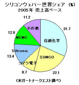
シリコンウェハーの2005年の世界シェアは添付の通りで、信越が32%、SUMCOが222%だが、SUMCOはコマツ電子の買収で合意しており、信越とSUMCOは拮抗することとなる。信越は今回の増設でSUMCOを突き放す。
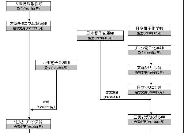
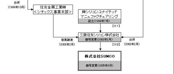
SUMCOは住友金属工業のシチックス事業本部(旧 住友シチックス、当初は大阪チタニウム)と三菱マテリアルシリコン(旧 チッソ電子化学+日本電子金属)が2002年に事業統合したもので、当初の社名は三菱住友シリコン。2005年8月に現社名に改称した。
両社は事業統合に先立ち、1999年に共同出資会社のシリコン・ユナイテッド・マニュファクチュアリング(SUMCO)を設立し,300mmウエハーの技術開発及び試作品用生産設備の管理・運営を共同で行った。現在の社名はこれを踏襲したもの。
シリコンウェハーの製造では米国に SUMCO Phoenix、SUMCO Southwest、フランスにSUMCO France、インドネシアに SUMCO Indonesia をもっている。
同社は2006年6月に、小松製作所の子会社(61.9%保有)のコマツ電子金属の株式総数の51%取得を目指すTOB実施を決めた。小松製作所は全所有株式でTOBに応募することを決めている。
コマツ電子金属は1960年の設立で、シリコンウェーハの製造・販売を業とし、長崎、宮崎、台湾に製造拠点を持っている。
台湾子会社は台湾小松電子材料で、コマツ電子金属が
51%、台湾プラスチックグループ が49%を出資し、麦寮の台塑工業園区に230億円を投じて月産10万枚の300mmシリコンウェハー工場を建設中。
SUMCOとコマツ電子金属はいずれもシリコンウェーハ専業メーカーで、大口径の300mmから小口径特殊品、高精度品までの幅広い事業分野をカバーしており、買収により、「相互に類似的、補完的な要素技術を持つ2社が、今後統合された事業戦略を共有化していくことにより、新しいSUMCOグループとして顧客の満足度を向上させていくことを目指す」としている。
Siltronic AGはWacker
Chemie の子会社でMunich
に本拠を置くシリコンウェーハ事業会社。ヨーロッパ、USA、東南アジア、日本の4大市場に工場を保有する。
工場はドイツのブルグハウゼン他2地区、米国ポートランド(オレゴン州)、シンガポール、マレーシア、光(山口県)にある。
光工場はワッカー・エヌエスシーイーの工場で、2000年に新日鐵100%子会社の旧ニッテツ電子にWacker
が55%出資した。
2003年にWacker
が顧客ニーズへの迅速な対応力を強化するために100%子会社とした。山口県光市とマレーシアのケタ州クリムに工場をもっている。
現在、Wacker が Siltronic を米国の投資会社 Francisco Partners に売却する交渉を行っているとの噂が流れている。.
MEMC
1959年にMonsanto
Chemical が米国でシリコン製造のためMonsanto Electronic Materials Company
を設立した。
欧州では1961年にDynamit
Nobel Silicon がイタリアにシリコン工場を建設している。
1989年にドイツのVEBAの子会社 Huls がMonsanto から同社を買収、別途1987年に買収したDynamit Nobel Silicon と合併させ、MEMC Electronic Materials, Inc とした。MEMCのブランドが有名なため、この名前を残した。
1995年にNew York で上場、その後もHuls は72%の株を持っていたが、Huls の親会社 VEBA が VIAG と統合して E. On になり、E. On は同社の売却を決め、2001年にTexas Pacific Groupに全持株を売却した。Texas Pacific はその後、大部分を売却し、25%を保有している。
MEMCは1991年に韓国で三星電子、Pohang Iron & Steel とのJVのPosco Huls を設立した。 2000年に MEMC はPohang Iron & Steel の持株を買収して80%の株主となり、社名をMEMC Korea Company.と改称した。
また、1994年には台湾で China Steel その他とのJV、Taisil Electronic Materials, Inc.を設立した。2005年には台湾初の300mm ウェーハをスタートさせた。
1995年にはTexas Instruments とのJV、MEMC Southwest, Inc.を設立し、Texas Instruments の既存プラントを活用している。
2006/9/20 300mmウエハー生産能力早期大幅増強を決定
全額出資子会社の信越半導体を通じ、デジタル家電や携帯電話などの半導体向けに需要が急伸しているシリコンウエハーの増産投資を実施。
(2007年秋に月産100万枚体制に)
300mmウエハー生産能力を今秋までに月産50万枚とする予定で増強
(信越化学 2004/12/22
信越半導体 300mmウエハー生産能力を国内外で大増設
http://www.shinetsu.co.jp/j/news/s20041222.shtml
信越化学工業株式会社(本社:東京、社長:金川千尋)の100%子会社である信越半導体株式会社(本社:東京、社長:秋谷文男)は、全世界の顧客に300mmシリコンウエハーを供給する世界最大のメーカーとして、国内外で大規模な投資を行い、2006年秋までにグループの生産能力を月産50万枚まで増設する計画を定め、その工事を開始した。今回の増設で信越半導体(株)は、全顧客の需要に応えると同時に300mmシリコンウエハーの世界No.1の座を揺るぎないものとする。
→ 前倒しで完了し、グループ全体で現在月産70万枚に引き上げた。
2007年秋には月産100万枚体制を構築する。
この30万枚の追加投資額は約1,200億円となり、この投資を含めた300mm事業への累積投資額は約4,000億円となる見込み。
主力の信越半導体㈱白河工場、
SEHアメリカ社、
グループ会社である三益半導体工業株式会社(本社:群馬県高崎市、社長:中澤正幸)
新たに長野電子工業株式会社(本社:長野県千曲市)で投資を行い、
これら4拠点を通じ需要家への安定供給を図る。
又、単結晶(インゴット)生産においても、リスク分散を図る為
既存の白河工場、
SEHアメリカ社の増強に加え、
信越半導体(株)武生工場(福井県越前市)でも生産
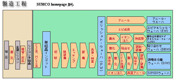
シリコンウエハーは高純度のシリコンの種結晶を円柱状に成長させたインゴットを薄くスライスした円盤状の
シリコンなどの半導体の素材の種結晶を円柱状に成長させたインゴットを薄くスライスした円盤状の板である。シリコンウェーハ業界ではウェハーではなくウェーハと呼ぶことが多い。
-----------
信越が約31%、三菱マテリアルと住友金属工業の事業統合会社であるSUMCOが約22%の世界シェアを握り、つばぜり合いを展開している。
SUMCOは約8%のシェアを持つコマツ電子の買収で合意している。信越は2工場新設で再びSUMCOを突き放す考え。両社の投資競争は取引先の投資や雇用も呼び起こしそうだ。
----------------
日本経済新聞 2005/10/15
300ミリウエハー SUMCO、生産能力2倍 月産70万枚に 2009年までに1300億円投資
三菱マテリアルと住友金属工業が共同出資するシリコンウエハー製造会社SUMCO(旧三菱住友シリコン)は2009年4月までに、直径300ミリウエハーの生産能力を現在の倍の月70万枚に引き上げる。今年度以降の投資総額は1300億円程度になる。
平成13年6月26日 公正取引委員会
住友金属工業(株)及び三菱マテリアル(株)によるシリコンウエハー事業の統合について
公正取引委員会は,住友金属工業(株)(以下「住友金属」という。)及び三菱マテリアル(株)(以下「三菱マテリアル」という。)から,両社が平成14年1月を目途に予定しているシリコンウエハーに係る事業の統合について事前相談があったので,その検討を行ってきた。
当委員会は,相談があった内容に関する当事会社の説明を前提とすれば,本件統合は独占禁止法の規定に違反するおそれはないものと認められる旨,当事会社に回答を行った。
1 本件の概要
(1) 本件は,住友金属,三菱マテリアル及びその100%子会社である三菱マテリアルシリコン(株)(以下「三菱MS」という。)が,経営資源の効率的利用等を目的として,次世代の300mmシリコンウエハー(以下「300mmウエハー」という。)を含め,両社のシリコンウエハー事業全体を統合しようとするものである。
(注) 住友金属,三菱マテリアル及び三菱MSは,平成11年3月,共同出資会社である㈱シリコン・ユナイテッド・マニュファクチュアリング(以下「SUMCO 」という。)を設立し,シリコンウエハーのうち次世代の300mmウエハーについて,技術開発及び試作品用生産設備の管理・運営を共同で行っている。(2)シリコンウエハーとは,半導体回路の基板となる円盤状の材料であり,ユーザーである半導体メーカーがこれを加工・切断して,ダイオード,トランジスタ,IC(集積回路),LSI(大規模集積回路)などの電子機器用のシリコンチップにしている。
現在のシリコンウエハーは,直径が150mm及び200mmのものが主力であるが,将来的には,200mmシリコンウエハーの2倍強のチップを生産でき,かつ,生産コストを大幅に削減できる300mmウエハーが主力となると見られており,現在,シリコンウエハーメーカー各社は,主に,ユーザーである半導体メーカー向けの試験用として300mmウエハーを生産している。
2 独占禁止法上の考え方
(1)一定の取引分野
本件においては,シリコンウエハーの製造・販売について,一定の取引分野が成立すると判断した。
(2)競争への影響
当事会社のシリコンウエハーの国内における販売金額シェアを合算すると約30%となり,その順位が第1位となる。
しかしながら,以下の事情を総合的に勘案すれば,本件統合により,(1)で画定した取引分野における競争を実質的に制限することとはならないと判断した。
ア 販売金額シェアで10%を超す競争業者が複数存在し,そのうち1社は20%を超す競争業者であること。また,複数の海外の有力メーカーが国内に参入し,生産拠点を持っていること
イ ユーザーは大手半導体メーカー等であり,その価格交渉力は強く,シリコンウエハー価格も年々下落傾向にあること
ウ ユーザーは,競争的価格での購入等を目的として,複数のメーカーからシリコンウエハーを購入していること【※1】1999年7月、住友金属工業(株)、三菱マテリアル(株)、三菱マテリアルシリコンの共同出資により、300mmシリコンウェーハの開発・製造会社として(株)シリコンユナイテッドマニュファクチュアリングが設立。
【※2】2002年2月、(株)シリコンユナイテッドマニュファクチュアリングが住友金属工業(株)よりシリコン事業の営業を譲渡するとともに、三菱マテリアルシリコン(株)と合併、同時に商号を三菱住友シリコン(株)に変更。
2006年06月16日
コマツがコマツ電子金属をSUMCOへ売却、SUMCOがTOBを実施
SUMCOは、小松製作所(コマツ)傘下のコマツ電子金属を対象とした株式公開買付け(TOB)を実施する。SUMCOは、コマツ電子金属の発行済み株式総数の51%(1540万2000株)取得を目指す。コマツはTOB応募に合意しており、SUMCOとコマツは6月14日に基本合意書を締結した。
SUMCOとコマツ電子金属はいずれもSiウェーハ専業メーカーで、大口径の300mmから小口径特殊品、高精度品までの幅広い事業分野をカバーしている。コマツ電子金属を買収することで、SUMCOは「相互に類似的、補完的な要素技術を持つSiのピュアプレーヤー2社が、今後統合された事業戦略を共有化していくことにより、新しいSUMCOグループとして顧客の満足度を向上させていくことを目指す」としている。コマツ電子金属にとっては、SUMCOグループの一員になることで、台湾における300mmウェーハの設備投資の加速や技術面でのシナジーが期待できるという。
今後SUMCOとコマツは基本合意書の内容に従い、詳細調査実施などの手続きを協力して進める。所要手続きが完了した後、TOBに関する契約を締結した上で、SUMCOはコマツ電子金属が発行する普通株式の51%をTOBで取得する予定だ。現在コマツは、コマツ電子金属の発行済み株式の61.93%に相当する1870万2900株を持っている。この全保有株式でTOBに応募する。
コマツ電子金属の概要]
商号:コマツ電子金属株式会社 (Komatsu Electronic
Metals Co. , Ltd.)
設立年月日:1960年4月18日
本店所在地:長崎県大村市雄ケ原町1324番地2
代表者:代表取締役社長 阿部 隆司
事業内容:シリコンウェーハの製造・販売
大株主:コマツ(61.9%)
生産拠点:長崎、宮崎、台湾(台湾小松電子材料股イ分有限公司)
従業員数:2,758人
売上高:866億円 (2006年3月期)
台湾子会社に300mmウェーハ工場を建設 平成17年1月14日
コマツ電子金属(社長 池田邦雄、本社 長崎県大村市)は、今般台湾プラスチックグループとの合弁会社である当社連結子会社の台湾小松電子材料股イ分有限公司(英語名略称:FKS)に、300mmウェーハ工場の建設を決定しました。
今般の決定内容は、現在200mmウェーハを生産しているFKSに、月産10万枚規模の300mmウェーハ工場棟を建設し、当初月産5万枚規模の一貫生産ラインを設置して、2006年内の稼動開始を目標とするもので、その後は需要動向を見極めながら生産能力を段階的に増強していく考えです。今般の投資額は、約230億円の予定です。
当社は、今後も300mmウェーハの需要拡大が見込まれることから、国内生産に加え、台湾に生産体制を構築し、当社グループとして300mmウェーハの供給能力増強を図り、顧客ニーズに対応していきます。
<FKSの概要>1)会社名 :台湾小松電子材料股イ分有限公司
2)英語名 :FORMOSA KOMATSU SILICON CORP.
3)設 立 :1995年11月21日
4)資本金 :42億6,875万新台湾ドル
5)出資比率:コマツ電子金属・・・51% 台湾プラスチックグループ・・・49%
6)代表者 :董事長:王 永慶 総経理:滝口 蓮一
7)所在地 :台湾雲林縣麦寮郷台塑工業園区10号
MEMC Electronic Materials, Inc.
1961
Dynamit Nobel Silicon (DNS) builds a plant in Merano, Italy. DNS
would later combine with Monsanto Electronic Materials Company to
form "MEMC" in 1989.
MEMC is a leading global supplier of wafers to the semiconductor industry. Wafers are the fundamental building block on which nearly all microelectronic applications are made. These applications, or “devices”, make possible the Internet and electronic commerce, computers, consumer electronics, automobiles, telecommunications, industrial automation and control systems, and analytical and defense systems.
MEMC operates nine manufacturing facilities in every key semiconductor region in the world, including Japan, Korea, Malaysia, Taiwan, Europe, and the United States. MEMC's diversity of manufacturing locations ensures a presence in all major semiconductor markets. This has been our strategy since the company's inception over 40 years ago as the first merchant manufacturer of silicon wafers in the world!
On August 6, 1959, St. Louis, Missouri-based Monsanto Chemical Company announced a new ultra-pure "Silicon Metal" electronics division. Construction began immediately on a manufacturing plant in rural St. Charles County, approximately 30 miles west of Monsanto headquarters. The plant was designed to produce silicon "used in the manufacture of transistors and rectifiers". The new business venture, Monsanto Electronic Materials Company, was a culmination of several years of research at two of Monsanto's labs in St. Louis and Dayton, Ohio.
According to the original press release, the rural location of the facility was chosen because, "The nature of ultra-pure silicon is such that it must be manufactured in an area where the atmosphere is free from even the slightest impurities". Today, the St. Peters plant is the largest of MEMC's facilities and serves as the corporate world headquarters. It is also serves as the world headquarters for MEMC's research and development.
The first silicon wafer produced in 1959 was 19mm in diameter!
The 1960's marked a period of steady growth for the company and solidified MEMC's reputation as a technology leader. It was a time of true pioneering work by MEMC scientists in electronic materials. In fact, much of their work remains an industry standard even today. One of these innovations was Chemical Mechanical Polishing. Wafer polishing quickly became a flatness standard because customers were striving for smaller, faster circuits. Over the course of the decade, one-inch wafers eventually gave way to 1.5" wafers. Epitaxial deposition made its first appearance at MEMC in 1966. However, the big story of the '60s, and widely considered a pioneering breakthrough in silicon materials science, was the discovery of Zero Dislocation silicon crystals by MEMC Fellow, Dr. Horst Kramer.
The fact that MEMC and the semiconductor industry experienced simultaneous and sustained growth during the 70's was no coincidence. As the demand for smaller, faster, integrated circuits surged, MEMC added capacity in 1970 with the construction of the Kuala Lumpur, Malaysia facility. Within a few years, MEMC would add crystal and polishing capacity at the St. Peters plant. The 70's were also about technology advancement, as wafer diameters progressed from 2.25" to 5" (125mm) in 1979. Throughout the decade, MEMC helped the silicon industry progress with further Chemical Mechanical Polishing, Zero-D crystal, and wafer flatness innovations.
In the 80's, MEMC continued to forge the technology roadmap. MEMC was the first to commercially introduce 150mm diameter wafers in 1981. A new, state-of-the-art, manufacturing facility was built in Spartanburg, South Carolina to handle the growing demand for silicon wafers. Then in 1982, MEMC pioneered Epi for CMOS applications, a major turning point in the semiconductor industry. By applying an epitaxial layer to the surface of a silicon wafer, MEMC made more advanced applications possible. In 1983, MEMC constructed the Utsunomiya, Japan plant, becoming the first non-Japanese wafer maker with manufacturing and research facilities in Japan. The following year, MEMC became the first wafer manufacturer to commercially produce 200mm diameter wafers, once again, an industry leader.
After 30 years as a division of agricultural and chemical giant Monsanto, the electronic materials division began a new era under the ownership of Huls AG, a subsidiary of VEBA AG. In April 1989, Huls consolidated the former Monsanto division with Dynamit Nobel Silicon Holdings, Inc. (DNS) which had been acquired by Huls in 1987. The new company name: MEMC Electronic Materials, Inc. The DNS Novara and Merano, Italy facilities became part of the MEMC family. The abbreviated moniker of Monsanto Electronic Materials Company, "MEMC", was retained due to brand name equity and customer recognition. A year later, the MEMC World Headquarters was moved from Palo Alto, California, to St. Peters, Missouri.
The new MEMC experienced explosive growth in the nineties through technological innovation and strategic partner alliances. In 1991, MEMC again demonstrated silicon leadership as one of the first wafer suppliers to manufacture 300mm wafers. That same year, the "Posco Huls Company" (PHC) joint venture was created between MEMC, Samsung Electronics, LTD and Pohang Iron & Steel Co., LTD. The Chonan facility was built to produce 200mm wafers primarily for the Korean market. Three years later, "Taisil Electronic Materials, Inc." (Taisil) was established as a joint venture in Taiwan between MEMC, China Steel, and others. Taisil built the facility in the Hsinchu Science Park in order to serve the growing Taiwan semiconductor market. In 1995, MEMC forged yet another strategic alliance with Texas Instruments called "MEMC Southwest, Inc.". MEMC Southwest began operations by utilizing an existing 6" TI facility. Several years later, 200mm capacity was added with a new, separate, state-of-the-art manufacturing facility.
Because polysilicon is the primary raw material for all silicon wafer manufacturers, MEMC purchased a granular polysilicon production facility from Albemarle Corporation and renamed the enterprise "MEMC Pasadena, Inc.", in 1995. Granular polysilicon provides inherent efficiencies and cost advantages over traditional chunk polysilicon. Furthermore, MEMC believes granular polysilicon has unique advantages in the production of 300mm wafers.
The highlight of the 1990's was MEMC stock trading on the New York Stock Exchange under "WFR". The Initial Public Offering on July 12, 1995 raised more than $440 million dollars in capital. VEBA AG retained a majority interest in MEMC following the IPO and throughout the 90's.
Unfortunately, and much like the entire semiconductor industry, MEMC experienced volatile and negative business conditions in 1998 and 1999. A severe drop in consumer electronics demand, coupled with worldwide over-capacity, forced MEMC (and the silicon industry) into a devastating downturn. However, MEMC survived one of the longest and most severe downturns in history with the title, "Biggest financial turnaround in electronic materials history", according to Rose Associates.
In 1999, parent company and largest shareholder VEBA AG, announced that it had merged with VIAG AG to form one of Europe's largest conglomerates, E.ON AG. In connection with the merger, E.ON decided to divest of all non-core businesses in order to focus on energy. Also in 1999, the Company received a record number of patents. Sixty-two patents were issued worldwide with half being issued in the United States. Two of the most important products developed and presented with base patents were MDZ, and Perfect SiliconTM. Perfect SiliconTM brand wafers are a breakthrough in silicon technology by eliminating crystal defects at the wafer surface and throughout the wafer bulk.
In October 2000, MEMC purchased the 40% interest in PHC from Pohang, Iron & Steel Company, increasing its ownership to 80%. As a result, the joint venture was re-named "MEMC Korea Company".
On November 13, 2001, Texas Pacific Group and its co-investors, entered into an agreement with E.ON AG to purchase E.ON's 72% interest in MEMC and all of E.ON's outstanding loans to MEMC. Founded in 1993, Texas Pacific Group is a private investment partnership with capital of more than $8 billion. The partnership also has close ties to the semiconductor industry. Other technology companies in their substantial portfolio are; On Semiconductor, Seagate, Globespan, and Gemplus. In addition, they also have invested in a much broader range of industries including, Del Monte Foods, J. Crew, Punch Taverns, Bally, Ducati Motorcycles, Oxford Health Plans, and Magellan Health Services. Together with TPG, our goal is to advance MEMC's global position and to secure our place amongst the leaders in the semiconductor industry.
On February 24, 2005, TPG Wafer Holdings LLC, completes the sale(s) of 85,000,000 shares of common stock. TPG's beneficial ownership of the company's common stock is reduced from 63% to approximately 25%.
On August 30, 2005, MEMC celebrated the start of 300mm wafer production at its Taisil facility in Hsinshu, Taiwan with a traditional "Ribbon Cutting" ceremony. MEMC now becomes the first producer of 300mm wafers in Taiwan.
Siltronic posts profit amid polysilicon boom
Mark LaPedus
EE Times
(03/17/2006 8:58 PM EST)
SAN JOSE, Calif. ? Amid strong demand for its polysilicon products in the solar market, Wacker-Chemie AG’s silicon wafer unit on Friday (March 17) said that it returned to profitability on growing sales for 2005.
The silicon wafer unit, Siltronic AG (Munich, Germany), reported an EBIT of 5.8 million euros ($7.1 million) in 2005, compared to a loss of 100.7 million euros ($122.8 million) in 2004.
Silitronic generated sales of 925 million euros ($1.1 billion) in 2005, up 13.7 percent from 813.7 million euros ($992.5 million) in 2004.
In the 300-mm wafer segment, the unit’s volume growth was far above the overall average at 69 percent. And it benefited from a series of cost-cutting measures over the years.
For example, the closure of two 200-mm production sites in 2003 and 2004 boosted capacity utilization rates at lines in Singapore, Hikari, Japan, and Portland, Ore., in 2005, according to the company. Another turnaround factor was the expansion of 300-mm capacity at its factory in Freiberg, Germany.
It’s been a topsy-turvy time for Siltronic, which shelved its initial public offering in Germany in 2004. Despite the growth, the company has been losing ground to other silicon wafer makers, including MEMC, SEH and SUMCO.
Wacker Chemie is also said to be in talks to sell its wafer making subsidiary, Siltronic, with U.S. investment firm Francisco Partners being among interested parties, according to a recent report.ーーー
2003/05/28
Wacker-Chemieグループによるワッカー・エヌエスシーイー社の完全子会社化について
Wacker-Chemie GmbH(以下「Wacker-Chemie」)グループは、新日本製鐵株式会社(以下「新日鐵」)が保有するワッカー・エヌエスシーイー株式会社(以下「WNC」)の株式全部(発行済株式総数の45%)を本年9月30日までに買い取ります。これによりWacker-ChemieグループがWNCの全株式を保有することとなります。
WNCは、平成12年11月に新日鐵の100%子会社であった旧ニッテツ電子株式会社にWacker-Chemieグループが資本参加し、同グループが55%、新日鐵が45%の株式を保有する合弁会社として発足しました。以来、WNCはWacker-Chemieグループとの間で技術、販売、研究・開発等の面において連携し、シナジー効果を享受してきましたが、シリコンウェーハ市場や顧客ニーズへの迅速な対応力を強化するためには、Wacker-ChemieグループがWNCの全株式を保有し、幅広い品揃えと全世界的な販売ネットワークをもつ同グループの一員として連携を一層強化することが必要となりました。
Wacker-Chemieグループは、今回の措置に合わせてWNCを含むシリコンウェーハ事業の生産ラインの最適化を図ることとしており、①WNC光工場の6インチウェーハラインの生産を来年央を目処に停止し、顧客の理解を得ながらWacker-Chemieグループの他の工場に注文を移管すると共に、②WNCマレーシアの8インチ生産工場の生産を本年内を目処に停止し、主に光8インチ工場に注文を集中させます。この一連の措置は、Wacker-Chemieが検討してきたシリコンウェーハ事業収益向上計画の一環をなすものであり、これにより、WNCのみならずシリコンウェーハ事業全体の稼動率向上を図り、需要動向に適応したより効率的な生産体制を確立することになります。
Wacker-Chemieグループは、日本市場の重要性を充分に認識し、今後ともWNCを通じて日本における事業基盤を強化・拡充していく方針であり、WNCはこうした方針のもとに、アルゴンアニール品や次世代を見据えて開発を進めているSOI (Silicon on Insulator)等の高付加価値商品の売上拡大を図ると共に、将来的には12インチウェーハのライン増強も視野にいれて積極的な事業展開を図っていきます。
新日鐵は、これまでも合弁パートナーとしてWNC事業に最大限の協力を行ってきましたが、WNCがWacker-Chemieグループの完全子会社となることが同社の更なる成長と発展のために必要で、新日鐵の経営資源戦略にも合致すると判断いたしました。
(連絡先) 新日本製鐵株式会社 総務部広報センター 中島(03-3275-5023)
ワッカー・エヌエスシーイー株式会社 総務部 和久田(0833-72-8406)
(参考)
1.ワッカー・エヌエスシーイー株式会社
代表取締役社長 Dr. Albrecht P. Mozer (アルブレヒト モッツアー)
資本金 135億円 (ワッカー55%、新日鐵45%)
総資産 450億円
本社 東京都中央区
従業員 約1千人
昨年売上高 約200億円
主要工場 光工場(山口県光市) 12インチライン, 8インチライン、6インチライン
マレーシア工場 (ケタ州クリム) 8インチライン
2.ワッカーケミー社(Wacker-Chemie GmbH)
CEO Dr. Peter Alexander Wacker (ピーター アレキサンダー ワッカー)
資本金 260.8百万ユーロ (約313億円 1ユーロ=120円で換算、以下同じ。)
総資産 2,762百万ユーロ (約3,310億円)
本社 ドイツ ミュンヘン市 (主要工場 ブルグハウゼン市 ミュンヘンより約150km東)
従業員 約17千人
昨年売上高 2,678百万ユーロ (約3,210億円)
事業内容 シリコンウェーハ、苛性ソーダ等化学品、シリコン樹脂・シリカ等のシリコン製品の製造販売
3.ワッカーシルトロニック社(Wacker Siltronic AG)
ワッカーケミー社のシリコンウェーハ事業を推進する100%子会社、ヨーロッパ、USA、東南アジア、日本の4大市場に工場を保有する。
CEO Dr. Wilhelm Sittenthaler (ウィルヘルム シッテンターラー)
資本金 100百万ユーロ (約120億円)
総資産 1,248百万ユーロ (約1,500億円)
本社 ドイツ ブルグハウゼン市
工場 ドイツ、ブルグハウゼン他2地区、
米国ポートランド(オレゴン州)、シンガポール、マレーシア、光(山口県)
従業員 約7千人
売上規模 1,017百万ユーロ (約1,220億円)WNC連結ベース
事業内容 シリコンウェーハ、多結晶シリコンの製造・販売