News Highlights
- To build advanced packaging facility for next-generation HBM, while collaborating with Purdue University for R&D
- Selects Indiana for strong support provided by the state and local government, infrastructure for manufacturing, and talent at Purdue
- Industry’s first investment in advanced packaging for AI products on American soil, strengthens supply-chain resilience
SK hynix Inc. , the world’s leading producer of High-Bandwidth Memory (HBM)1 chips, announced today that it will invest an estimated $3.87 billion in West Lafayette, Indiana to build an advanced packaging fabrication and R&D facility for AI products. The project, the first of its kind in the United States, is expected to drive innovation in the nation’s AI supply chain, while bringing more than a thousand new jobs to the region.
1HBM (High Bandwidth Memory): A high-value, high-performance memory that vertically interconnects multiple DRAM chips and dramatically increases data processing speed in comparison with conventional DRAM products. HBM4 is the sixth generation of its kind, following HBM, HBM2, HBM2E, HBM3 and HBM3E.
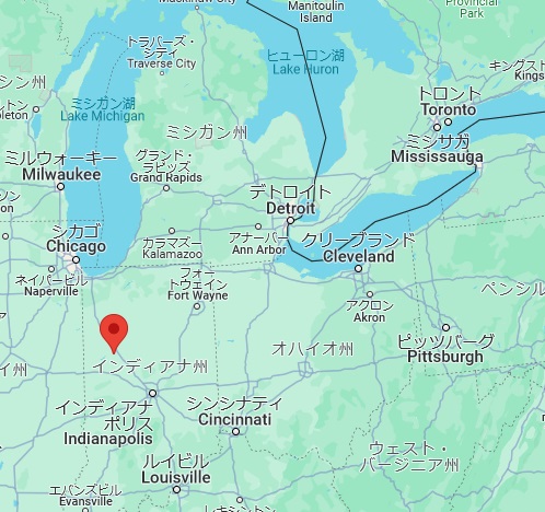
The company held an investment agreement ceremony with officials from Indiana State, Purdue University, and the U.S. government at Purdue University in West Lafayette on the 3rd and officially announced the plan.
At the event, officials from each party including Governor of Indiana Eric Holcomb, Senator Todd Young, Director of the White House Office of Science and Technology Policy Arati Prabhakar, Assistant Secretary of Commerce Arun Venkataraman, Secretary of Commerce State of Indiana David Rosenberg, Purdue University President Mung Chiang, Chairman of Purdue Research Foundation Mitch Daniels, Mayor of city of West Lafayette Erin Easter, Ambassador of the Republic of Korea to the United States Hyundong Cho, Consul General of the Republic of Korea in Chicago Junghan Kim, SK vice chairman Jeong Joon Yu, SK hynix CEO Kwak Noh-Jung and SK hynix Head of Package & Test Choi Woojin, participated.
Leveraging its dominant position in the HBM market, SK hynix’s new facility will be home to an advanced semiconductor production line that will mass-produce next-generation HBM, the highest-performing Dynamic Random Access Memory (DRAM) chips, which are the critical components of graphic processing units that train AI systems such as ChatGPT.
The company plans to begin mass production in the second half of 2028, while the new facility will also develop future generations of chips and house an advanced packaging R&D line. The site was selected due to Indiana’s resilient manufacturing infrastructure and R&D ecosystem, expert intellectuals in the semiconductor field and the talent pipeline at Purdue University, and the strong support provided by the state and local government.
Innovation in memory chips continues to drive lower-power operations and performance enhancements in computing. As tech shrinkage and other hardware improvements have hit limits, SK hynix’s new chiplet packaging technology has emerged as a promising way to continue enhancing density and performance. As this heterogeneous integration technology becomes more and more important to the future of the semiconductor industry, the company’s new initiative in Indiana will help establish the region as a Silicon Heartland: a new semiconductor cluster centered in the Midwest Triangle that will become a magnet for next-generation computing in the AI era.
“Indiana is a global leader in innovating and producing the products that will power our future economy, and today’s news is proof positive to that fact,” said Governor Eric Holcomb. “I’m so proud to officially welcome SK hynix to Indiana, and we’re confident this new partnership will enhance the Lafayette-West Lafayette region, Purdue University and the state of Indiana for the long term. This new semiconductor innovation and packaging plant not only reaffirms the state’s role in the hard tech sector, but is also another tremendous step forward in advancing U.S. innovation and national security, putting Hoosiers at the forefront of national and global advancements.”
U.S. Senator Todd Young, a key advocate for the project, said, “SK hynix will soon be a household name in Indiana. This incredible investment demonstrates their confidence in Hoosier workers, and I’m excited to welcome them to our state.” Adding, “The CHIPS and Science Act opened a door that Indiana has been able to sprint through, and companies like SK hynix are helping to build our high-tech future.”
“SK hynix is the global pioneer and dominant market leader in memory chips for AI,” Purdue University President Mung Chiang said. “This transformational investment reflects our state and university’s tremendous strength in semiconductors, hardware AI, and hard tech corridor. It is also a monumental moment for completing the supply chain of digital economy in our country through chips advanced packaging. Located at Purdue Research Park, the largest facility of its kind at a U.S. university will grow and succeed through innovation.”
“We are excited to become the first in the industry to build a state-of-the-art advanced packaging facility for AI products in the United States that will help strengthen supply-chain resilience and develop a local semiconductor ecosystem,” said SK hynix CEO Kwak Noh-Jung. “With this new facility, we hope to advance our goal of providing AI memory chips with unmatched capabilities, serving the needs of our customers.”
“We are grateful for the support from the Government of Indiana, Purdue University, and the broader community involved, and we look forward to expanding our partnership in the long run.”
As a technology leader, integrator, and enabler in memory solutions, SK hynix is collaborating with Purdue University, one of the leading research institutions in the U.S., on plans for future R&D projects. These projects include work on advanced packaging and heterogeneous integration with Purdue’s Birck Nanotechnology Center and other research institutes and industry partners. They also hope to collaborate on a project related to memory-centric solutions and architecture for the generative AI era, specifically system-level memory design and in/near-memory computing.
The company also plans to collaborate with Purdue University and Ivy Tech Community College to develop training programs and interdisciplinary degree curricula that will cultivate a high-tech workforce and build a reliable pipeline of new talent.
Meanwhile, SK hynix plans to support the work of Purdue Research Foundation and other local non-profits and charities by building partnerships that provide community development, growth opportunities, and leadership training.
Separately, SK hynix will also proceed with Korean domestic investments as planned. The company has been working to prepare the site for the Yongin Semiconductor Cluster where it will invest 120 trillion won to build production facilities. The company plans to break ground on the first fab in March of 2025, with plans for completion in early 2027. It will also build a mini fab, a facility with equipment for 300mm wafer processing, to test semiconductor materials, components and equipment.